

 English
WT9932S31-TINY Board Features
Update history
| Date | Version | Author | Update content |
|---|---|---|---|
| 2026-10-25 | 1.0.1 | YobieZhou | Added the corresponding English documentation |
| 2026-10-23 | 1.0.0 | YobieZhou | Added the board introduction, hardware peripherals, interface pin descriptions, and power characteristics |
Note: Disconnect power before connecting a camera. Check the pin sequence, contact side, cable orientation, and supply voltage of the
24Pin DVP FPCconnector. The same number of pins does not guarantee electrical compatibility.
1. Introduction
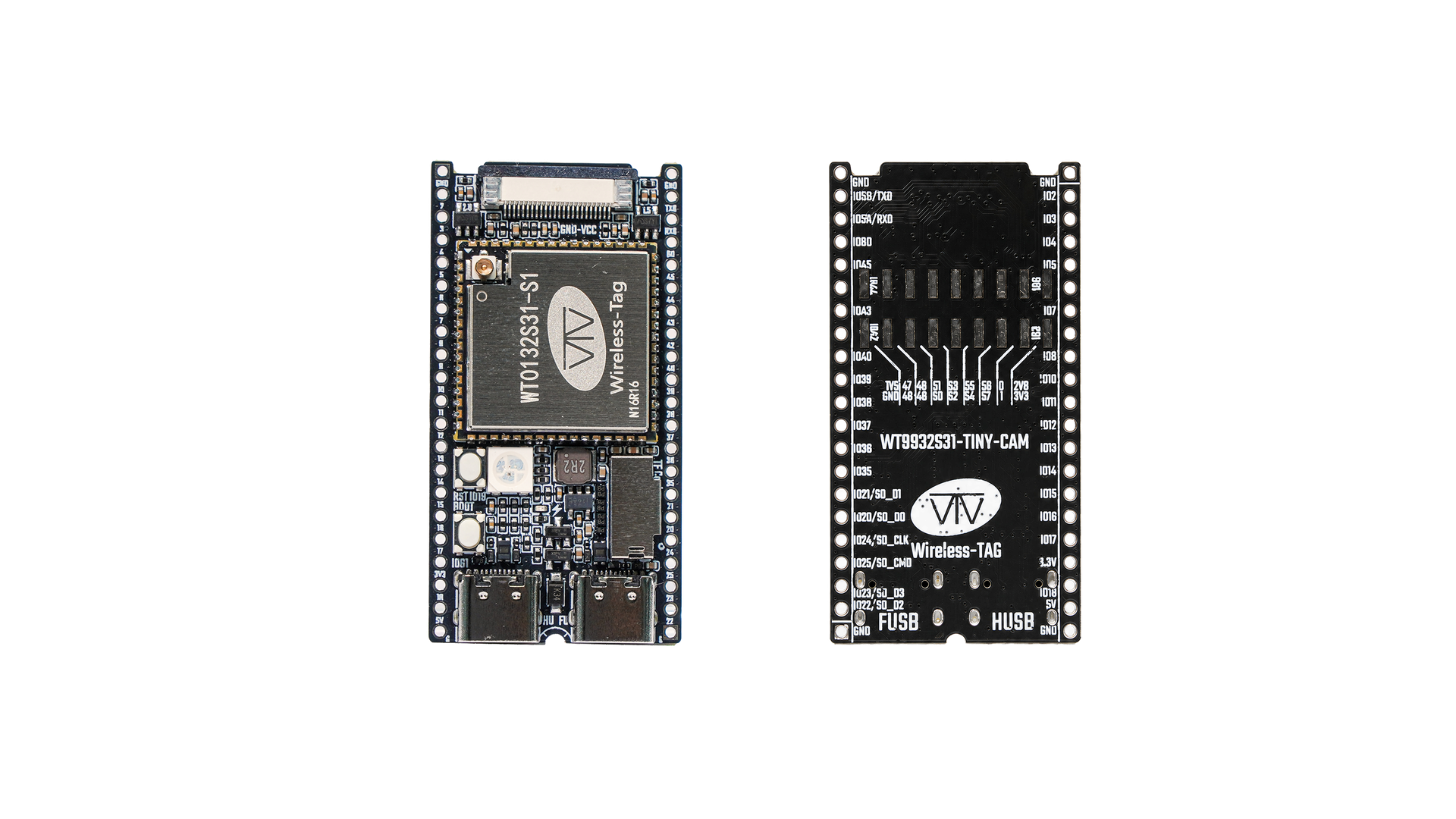
WT9932S31-TINY is a compact development board in Wireless-tag's TINY series. It is based on the WT0132S31-S1 module with Espressif's ESP32-S31 at its core, uses a four-layer PCB, and measures approximately 54 × 28 mm. The board combines wireless connectivity, camera capture, storage, and general-purpose peripheral expansion in a small footprint, making it suitable for space-constrained embedded applications and prototyping.
ESP32-S31 features a dual-core RISC-V processor running at up to 320 MHz and supports 2.4 GHz Wi-Fi 6, Bluetooth Low Energy, Bluetooth Classic, Zigbee, and Thread. The board provides 16 MB Flash and 32 MB PSRAM, an onboard DVP camera interface, a four-line MicroSD card slot, an RGB indicator, EN/RESET and BOOT buttons, and two USB Type-C ports labeled FUSB and HUSB. These resources support image capture, data storage, and evaluation of multiprotocol IoT applications.
1.1 Core Hardware Configuration
- Core module: Wireless-tag
WT0132S31-S1. - Main processor: Espressif
ESP32-S31, dual-coreRISC-V, running at up to320 MHz. - Memory:
16 MB Flashand32 MB PSRAM. - Wireless connectivity:
2.4 GHz Wi-Fi 6, Bluetooth Low Energy, Bluetooth Classic,Zigbee, andThread, with an external antenna connected through the module's RF interface. - Camera interface: A
24PinDVP FPCconnector with0.5 mmpitch, designed for theOV3660pin sequence;2 × 9DVPexpansion header pads with2.54 mmpitch are provided on the back. - Storage interface: An insertion/removal-type
MicroSD/TFcard slot supporting4-bitmode. - Pin headers: Two
21Pinheaders,H1andH2, with2.54 mmpitch for connection to breadboards or perfboards. - Debugging resources:
USB Serial/JTAG, high-speedUSB 2.0 OTG,UART0, anRGB LED, and reset and download-mode buttons. - Power design: Power combining and reverse-current protection for the two
USB Type-Cinputs, an onboard3.3 V DC-DCconverter, and2.8 Vand1.5 V LDOregulators for the camera. - Board dimensions: Approximately
54 × 28 mm; use the CAD files and 3D model for assembly dimensions.
1.2 Design Features
- High performance in a compact size: The
WT0132S31-S1module forms the core system, while the four-layerPCBbalances a compact layout with peripheral expansion. - DVP image capture: The onboard camera
FPCconnector accepts a compatible camera module for image capture, processing, and video transmission development. - Shared DVP and GPIO expansion: The
U5pads on the back have no pin header fitted by default. When no camera is used, a header can be soldered to use the corresponding signals for general-purpose peripheral expansion. - Dual USB ports:
J2/FUSBis used for firmware flashing, logging, andJTAGdebugging;J1/HUSBis used for high-speedUSBapplication development. - Onboard storage and interaction: The
MicroSDcard slot supports data logging, while theRGBindicator andBOOTbutton provide status indication and basic interaction. - Breadboard-friendly headers: The headers on both sides use
2.54 mmpitch for quick connection to sensors, control devices, or a custom carrier board. - Convenient mounting: Mounting features along the board edges support installation with retaining plates, screws, or a custom base.
1.3 Applications
- IoT devices: Evaluate wireless applications using
Wi-Fi, Bluetooth, and802.15.4, connect sensors, and implement device control. - Image capture and vision prototypes: Connect a compatible
DVPcamera for image capture,USBvideo transmission, and evaluation of vision applications. - Data logging: Use a
MicroSDcard to save captured data, logs, or application files. - Education and prototyping: Support embedded systems education, maker projects, customer solution evaluation, and custom carrier board development.
1.4 Development Advantages
- The module integrates the core system and RF circuitry, allowing the development board design to serve as a reference for further development.
- The hardware design is published on JLC's OSHWHub open-source hardware platform.
WT_BSPprovides board support and peripheral examples for the software. - Start with basic examples such as
RGB, buttons, andSDMMC, then evaluate camera andUSBapplications. See Board Resources for the relevant links.
2. Hardware Peripherals
| Peripheral | Description |
|---|---|
RGB LED |
WS2812-compatible single-wire indicator connected to IO19 |
SW1/RESET |
Connected to EN to reset the board |
SW2/BOOT |
Connected to IO61 to enter download mode; can also serve as a user button after the application starts |
J1/HUSB |
High-speed USB 2.0 OTG port with a maximum theoretical transfer rate of 480 Mbps |
J2/FUSB |
Full-speed USB Serial/JTAG port with a maximum theoretical transfer rate of 12 Mbps, used for flashing and debugging |
FPC2 |
24Pin DVP camera connector with 0.5 mm pitch |
CARD1 |
Insertion/removal-type MicroSD/TF card slot supporting four-line mode |
H1, H2 |
Two 21Pin expansion headers with 2.54 mm pitch |
U5 |
2 × 9 DVP expansion header pads with 2.54 mm pitch on the back; no header fitted by default |
2.1 Components
| Reference | Component | Description |
|---|---|---|
J1 |
High-speed USB 2.0 Type-C port |
Labeled HUSB and connected to high-speed USB OTG; accepts power input and supports application communication, but cannot supply power to external devices. |
J2 |
USB Serial/JTAG Type-C port |
Labeled FUSB; used for power input, firmware flashing, log output, and JTAG debugging. |
H1, H2 |
Expansion headers | Expose general-purpose GPIO, UART0, SD signals, and power for prototype connections. |
FPC2 |
DVP FPC connector |
Drawer-type, bottom-contact, 24Pin connector with 0.5 mm pitch, designed for the OV3660 pin sequence. |
CARD1 |
MicroSD/TF card slot |
Insertion/removal-type slot supporting a 4-bit SD bus for file storage and data logging. |
U5 |
DVP expansion header pads |
Expose camera signals and the 2.8 V, 3.3 V, and 1.5 V supplies; no pin header fitted at the factory. |
2.2 Connector Footprints
| Interface | Footprint | Notes |
|---|---|---|
H1, H2 headers |
HDR-TH_21P-P2.54-V-M |
21Pin, 2.54 mm pitch |
DVP FPC connector |
FPC-SMD_AFC07-S24FCA-00 |
Check cable orientation, contact side, and power pin sequence |
MicroSD/TF card interface |
TF-SMD_TF-021B-H265 |
Insertion/removal-type card slot on the front |
DVP expansion header |
HDR-SMD_18P-P2.54-H-M-R2-C18-LS17.0 |
2 × 9; no header fitted by default |
3. Pin Descriptions
3.1 H1 Header
H1 is a 21Pin header with 2.54 mm pitch. The H1 and H2 tables below list positions from top to bottom in the front-facing orientation shown in the pinout diagram on the resources page. "Position" identifies locations in the diagram; also refer to the schematic for connector pad numbers.
| Position | Pin | Description | Voltage Range | Notes |
|---|---|---|---|---|
| 1 | GND |
Power ground | 0 V |
|
| 2 | IO2 |
General-purpose input/output | 0 V/3.3 V |
|
| 3 | IO3 |
General-purpose input/output | 0 V/3.3 V |
|
| 4 | IO4 |
General-purpose input/output | 0 V/3.3 V |
|
| 5 | IO5 |
General-purpose input/output | 0 V/3.3 V |
|
| 6 | IO6 |
General-purpose input/output | 0 V/3.3 V |
|
| 7 | IO7 |
General-purpose input/output | 0 V/3.3 V |
|
| 8 | IO8 |
General-purpose input/output | 0 V/3.3 V |
|
| 9 | IO9 |
General-purpose input/output | 0 V/3.3 V |
|
| 10 | IO10 |
General-purpose input/output | 0 V/3.3 V |
|
| 11 | IO11 |
General-purpose input/output | 0 V/3.3 V |
|
| 12 | IO12 |
General-purpose input/output | 0 V/3.3 V |
|
| 13 | IO13 |
General-purpose input/output | 0 V/3.3 V |
|
| 14 | IO14 |
General-purpose input/output | 0 V/3.3 V |
|
| 15 | IO15 |
General-purpose input/output | 0 V/3.3 V |
|
| 16 | IO16 |
General-purpose input/output | 0 V/3.3 V |
|
| 17 | IO17 |
General-purpose input/output | 0 V/3.3 V |
|
| 18 | 3.3V |
Power output | 3.3 V |
Must not be used as a power input |
| 19 | IO18 |
General-purpose input/output | 0 V/3.3 V |
|
| 20 | 5V |
Power output | 5 V |
Must not be used as a power input |
| 21 | GND |
Power ground | 0 V |
3.2 H2 Header
H2 is a 21Pin header with 2.54 mm pitch. TX0 and RX0 correspond to IO58 and IO59, respectively; IO20 through IO25 are shared with the onboard MicroSD card slot.
| Position | Pin | Description | Voltage Range | Notes |
|---|---|---|---|---|
| 1 | GND |
Power ground | 0 V |
|
| 2 | IO58/TX0 |
UART0 TX / general-purpose input/output |
0 V/3.3 V |
Default serial transmit pin |
| 3 | IO59/RX0 |
UART0 RX / general-purpose input/output |
0 V/3.3 V |
Default serial receive pin |
| 4 | IO60 |
General-purpose input/output | 0 V/3.3 V |
strapping pin |
| 5 | IO45 |
General-purpose input/output | 0 V/3.3 V |
|
| 6 | IO44 |
General-purpose input/output | 0 V/3.3 V |
|
| 7 | IO43 |
General-purpose input/output | 0 V/3.3 V |
|
| 8 | IO42 |
General-purpose input/output | 0 V/3.3 V |
|
| 9 | IO40 |
General-purpose input/output | 0 V/3.3 V |
|
| 10 | IO39 |
General-purpose input/output | 0 V/3.3 V |
|
| 11 | IO38 |
General-purpose input/output | 0 V/3.3 V |
|
| 12 | IO37 |
General-purpose input/output | 0 V/3.3 V |
strapping pin |
| 13 | IO36 |
General-purpose input/output | 0 V/3.3 V |
strapping pin |
| 14 | IO35 |
General-purpose input/output | 0 V/3.3 V |
|
| 15 | IO21 |
SD DATA1 / general-purpose input/output |
Depends on SD I/O configuration |
Shared with the card slot |
| 16 | IO20 |
SD DATA0 / general-purpose input/output |
Depends on SD I/O configuration |
Shared with the card slot |
| 17 | IO24 |
SD CLK / general-purpose input/output |
Depends on SD I/O configuration |
Shared with the card slot |
| 18 | IO25 |
SD CMD / general-purpose input/output |
Depends on SD I/O configuration |
Shared with the card slot |
| 19 | IO23 |
SD DATA3 / general-purpose input/output |
Depends on SD I/O configuration |
Shared with the card slot |
| 20 | IO22 |
SD DATA2 / general-purpose input/output |
Depends on SD I/O configuration |
Shared with the card slot |
| 21 | GND |
Power ground | 0 V |
Note:
IO36,IO37,IO60, andIO61are chip boot configuration pins. External circuitry must maintain the correct levels when these pins are sampled at startup.IO61is connected to the onboardBOOTbutton.
3.3 J1 and J2 USB Type-C Ports
| Port | Board Label | Function | Maximum Theoretical Transfer Rate | Power |
|---|---|---|---|---|
J1 |
HUSB |
High-speed USB 2.0 OTG for camera and other USB applications |
480 Mbps |
Accepts power input; cannot supply power to external devices |
J2 |
FUSB |
USB Serial/JTAG for firmware flashing, log output, and debugging |
12 Mbps |
Accepts power input |
When both ports are connected, the power combining circuit gives priority to J2/FUSB. When developing USB Host applications with J1, provide a separate power solution appropriate for the peripheral.
3.4 CARD1 MicroSD/TF Card Interface
CARD1 is an insertion/removal-type card slot supporting 4-bit mode. The card slot supply is 3.3 V.
| No. | Pin | Description | Voltage Range |
|---|---|---|---|
| 1 | IO22 |
SD DATA2 |
Depends on SD I/O configuration |
| 2 | IO23 |
SD DATA3 |
Depends on SD I/O configuration |
| 3 | IO25 |
SD CMD |
Depends on SD I/O configuration |
| 4 | VCC |
Card slot power supply | 3.3 V |
| 5 | IO24 |
SD CLK |
Depends on SD I/O configuration |
| 6 | GND |
Power ground | 0 V |
| 7 | IO20 |
SD DATA0 |
Depends on SD I/O configuration |
| 8 | IO21 |
SD DATA1 |
Depends on SD I/O configuration |
The accompanying WT_BSP SDMMC configuration uses the on-chip LDO 1 to configure the SD I/O supply as 1.8 V. Verify the card slot supply and the controller's signal supply configuration separately; the signal levels cannot be inferred from the card slot VCC alone. Before reassigning IO20 through IO25 to other functions, check the chip power domain, software configuration, and voltage-level requirements of the connected devices.
3.5 FPC2 DVP Camera Interface
FPC2 is a drawer-type, bottom-contact, 24Pin camera connector with 0.5 mm pitch, designed for the OV3660 pin sequence. The directions of the data and timing signals below are relative to the main controller. Camera signals Y2 through Y9 correspond to the controller's eight-bit image data input.
| No. | Pin | Description | Voltage Range | Notes |
|---|---|---|---|---|
| 1 | NC |
Not connected | — | Leave unconnected |
| 2 | 3.3V |
Camera power output | 3.3 V |
|
| 3 | Y4 |
Parallel image data | 0 V/3.3 V |
IO48, input |
| 4 | Y3 |
Parallel image data | 0 V/3.3 V |
IO47, input |
| 5 | Y5 |
Parallel image data | 0 V/3.3 V |
IO49, input |
| 6 | Y2 |
Parallel image data | 0 V/3.3 V |
IO46, input |
| 7 | Y6 |
Parallel image data | 0 V/3.3 V |
IO50, input |
| 8 | PCLK |
Camera pixel clock | 0 V/3.3 V |
IO54, input |
| 9 | Y7 |
Parallel image data | 0 V/3.3 V |
IO51, input |
| 10 | GND |
Power and signal ground | 0 V |
|
| 11 | Y8 |
Parallel image data | 0 V/3.3 V |
IO52, input |
| 12 | XMCLK |
Master clock output to the camera | 0 V/3.3 V |
IO55, output |
| 13 | Y9 |
Parallel image data | 0 V/3.3 V |
IO53, input |
| 14 | 2.8V |
Camera power output | 2.8 V |
|
| 15 | 1.5V |
Camera digital core power output | 1.5 V |
|
| 16 | HREF |
Line-valid signal | 0 V/3.3 V |
IO57, input |
| 17 | PWDN |
Camera standby control, active high | 0 V/3.3 V |
Pulled down on the board by default |
| 18 | VSYNC |
Frame synchronization signal | 0 V/3.3 V |
IO56, input |
| 19 | RESET |
Camera hardware reset, active low | 0 V/3.3 V |
Pulled up on the board by default |
| 20 | I2C_SCL |
Camera SCCB configuration clock |
0 V/3.3 V |
IO1, output |
| 21 | GND |
Power and signal ground | 0 V |
|
| 22 | I2C_SDA |
Camera SCCB configuration data |
0 V/3.3 V |
IO0, bidirectional |
| 23 | GND |
Power and signal ground | 0 V |
|
| 24 | NC |
Not connected | — | Leave unconnected |
PWDN and RESET have fixed bias levels provided by the onboard circuitry and are not connected to GPIO pins that software can control directly. The accompanying software supports compatible GC2145 and OV3660 camera configurations. Select the driver or firmware that matches the camera actually connected.
3.6 U5 DVP Expansion Header
U5 consists of 2 × 9 horizontal surface-mount header pads with 2.54 mm pitch; no header is fitted by default. Its signals are shared with FPC2. Before connecting peripherals, ensure that they and the camera will not drive the same signal simultaneously.
| No. | Pin | Description | Voltage Range |
|---|---|---|---|
| 1 | 2.8V |
Power output | 2.8 V |
| 2 | 3.3V |
Power output | 3.3 V |
| 3 | IO0 |
Camera SCCB SDA / general-purpose input/output |
0 V/3.3 V |
| 4 | IO1 |
Camera SCCB SCL / general-purpose input/output |
0 V/3.3 V |
| 5 | IO56 |
DVP VSYNC / general-purpose input/output |
0 V/3.3 V |
| 6 | IO57 |
DVP HREF / general-purpose input/output |
0 V/3.3 V |
| 7 | IO55 |
DVP XMCLK / general-purpose input/output |
0 V/3.3 V |
| 8 | IO54 |
DVP PCLK / general-purpose input/output |
0 V/3.3 V |
| 9 | IO53 |
DVP Y9 / general-purpose input/output |
0 V/3.3 V |
| 10 | IO52 |
DVP Y8 / general-purpose input/output |
0 V/3.3 V |
| 11 | IO51 |
DVP Y7 / general-purpose input/output |
0 V/3.3 V |
| 12 | IO50 |
DVP Y6 / general-purpose input/output |
0 V/3.3 V |
| 13 | IO49 |
DVP Y5 / general-purpose input/output |
0 V/3.3 V |
| 14 | IO48 |
DVP Y4 / general-purpose input/output |
0 V/3.3 V |
| 15 | IO47 |
DVP Y3 / general-purpose input/output |
0 V/3.3 V |
| 16 | IO46 |
DVP Y2 / general-purpose input/output |
0 V/3.3 V |
| 17 | 1.5V |
Power output | 1.5 V |
| 18 | GND |
Power and signal ground | 0 V |
4. Power Characteristics
Power the development board through either J2/FUSB or J1/HUSB.
- Use a good-quality
USB-Ccable that supports data transfer. - When powering the board from a computer's
USBport, a port capable of supplying at least5 V/1 Ais recommended. - Both
USBports have power combining and reverse-current protection. When both are connected,J2/FUSBhas priority. - The onboard
DC-DCconverter converts the input supply to3.3 Vfor the module and related peripherals. The camera circuitry has separate2.8 Vand1.5 V LDOregulators. - The
5Vand3.3Vpins onH1are power outputs and must not be used as external power inputs. - The power pins on
U5andFPC2are outputs at their respective voltages. Check the power direction before connecting expansion peripherals to avoid shorting different power nets together. J1/HUSBcannot supply power to external devices. If aUSBperipheral requires power, design a separate power solution based on the actual circuit.- The
MicroSDcard slot supply is3.3 V. See the interface description above for the software configuration of theSD I/Osupply.