English
WTDKP4C5-S1 Feature Introduction
Update history
| Date | Version | Author | Update content |
|---|---|---|---|
| 2025-12-3 | 1.0.0 | Pail | Initial document release |
1. Introduction
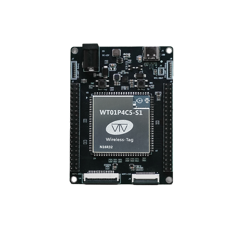
WTDKP4C5-S1 is a high-performance multimedia development board launched by wireless-tag, designed based on Espressif’s ESP32-P4 (RISC-V dual-core processor, 400 MHz) and ESP32-C5 (2.4G & 5G dual-band Wi-Fi 6 SoC). The core module model is WT01P4C5-S1. This development board focuses on MIPI-CSI and MIPI-DSI multimedia interfaces as well as dual-band Wi-Fi applications. It is suitable for smart home control, industrial HMI, medical devices, security monitoring, and multimedia terminals. Emphasizing low cost, low power consumption, and high integration, it is ideal for rapid prototyping of products such as IPC and AIoT.
Buy Now: WTDKP4C5-S1 Development Kit
Development Board Component Overview
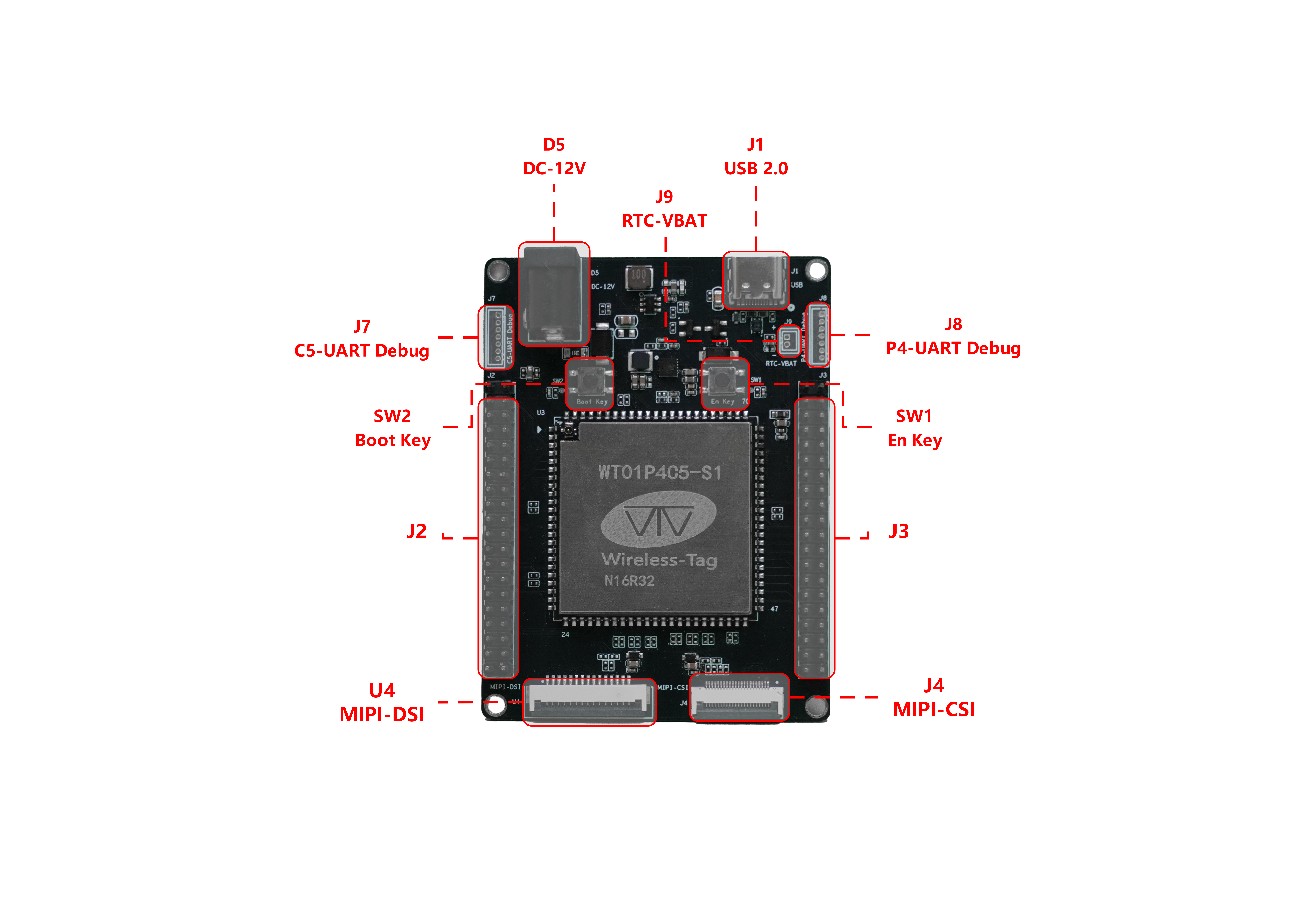
| Main Component | Ref. | Description |
|---|---|---|
| DC-12V | D5 | DC 12V power input |
| RTC-VBAT(NC) | J9 | Real-time clock power interface (NC) |
| USB 2.0 | J1 | USB 2.0 interface connected to the ESP32-P4 USB 2.0 OTG High-Speed port on the WT01P4C5-S1 core board. Supports USB 2.0 standard and can operate as a USB Device when connected to a USB Host. This port can also be used to power the board. |
| P4-UART Debug | J8 | P4 UART debug interface, connected to ESP32-P4 via UART. Works with wireless-tag flashing tools for viewing logs or flashing firmware to ESP32-P4. |
| En Key | SW1 | Reset button |
| J3 | J3 | Some available pins of WT01P4C5-S1 core board are routed to header J3. See details in the Pin Description. |
| MIPI-CSI | J4 | MIPI CSI FPC connector for camera modules. Supported FPC spec: 0.5 mm pitch, 0.3 mm thickness, 22 pins. |
| MIPI-DSI | U4 | MIPI DSI FPC connector for LCD extension boards. Supported FPC spec: 1 mm pitch, 0.3 mm thickness, 15 pins. |
| J2 | J2 | Some available pins of WT01P4C5-S1 core board are routed to header J2. See details in the Pin Description. |
| Boot Key | SW2 | Boot mode button. Hold BOOT and press EN to reboot WT01P4C5-S1 into "firmware download" mode, allowing firmware flashing to ESP32-P4 through USB 2.0. |
| C5-UART Debug | J7 | C5 UART debug interface, connected to ESP32-C5 via UART. Works with wireless-tag flashing tools for viewing logs or flashing firmware to ESP32-C5. |
🔧 Core Hardware Configuration
Main Controller: Espressif
ESP32-P4, featuring aRISC-V 400MHzhigh-performance processor and multiple multimedia subsystems, including aJPEG codec,pixel processing accelerator,H.264 encoder, andMIPI interfaces.Communication Chip: Espressif
ESP32-C5, supporting2.4G & 5G dual-band Wi-Fi 6,BLE5,Zigbee,Thread, andMatter.Multimedia Interfaces: Native support for
MIPI-CSIandMIPI-DSI.
MIPI-CSIconnects to MIPI camera modules, supporting2-lane × 1.5Gbps;
MIPI-DSIconnects to MIPI display modules, supporting2-lane × 1.5Gbps.Power Input:
Includes a12V DCinput connector for direct powering.
Also supports powering via the onboardType-Cconnector (5V).
🛠️ Design Features
- Dual-chip architecture:
ESP32-P4+ESP32-C5, connected viaSDIO, delivering both high-performance processing and high-speed wireless communication. - High-speed
USB 2.0 Type-Cinterface, fully supported byESP-IDF. MIPI CSI FPCconnector (0.5mm pitch, 22 pins) for image input.MIPI DSI FPCconnector (1.0mm pitch, 15 pins) for LCD output.
📡 Primary Application Scenarios
Data Acquisition:
58 general-purpose GPIOs (46 from ESP32-P4, 12 from ESP32-C5).
Flexible mapping toSPI,I2C,I2S, etc.
Built-inADC/DACand temperature sensors, supporting various external sensors.Industrial Control:
Dual-band Wi-Fi 6ensures reliable long-distance data transmission.
Optional Ethernet expansion via pin headers forWi-Fi to Ethernetgateway scenarios.HMI Interfaces:
Supports up to 7-inchMIPIorRGBdisplays + capacitive touch for local UI development (e.g., usingLVGL).Security & Vision Processing:
Multiple camera interfaces (MIPI-CSI/DVP/USB) supporting1080P@30fps.
Combined with ESP32-P4’s400MHz RISC-Vcore and ESP-WHO algorithms for edge AI tasks (e.g., face recognition).
⚙️ Development Advantages
- Both
ESP32-P4andESP32-C5support development via Espressif’s officialESP-IDF. - Official basic examples included for easy reference.
- wireless-tag’s GitHub provides multiple working examples for
MIPI-DSI,MIPI-CSI, etc., ready to download and flash.
2. Pin Description
The following table lists the names and function descriptions of the J2 pin header of the development board.
| Name | Function |
|---|---|
| IVCC_3V3 | 3.3V power input |
| C5_IO1 | GPIO1, LP_GPIO1, XTAL_32K_N, LP_UART_DSRN, ADC1_CHO |
| VCC_3V3 | 3.3V power input |
| C5_IO2 | GPIO1, LP_GPIO1, XTAL_32K_N, LP_UART_DSRN, ADC1_CHO |
| C5_EN | Enable ESP32-C5 chip (10K pull-up inside core module) |
| GND | Ground |
| C5_IO28_BOOT | GPIO28 |
| GND | Ground |
| C5_U0TXD | GPIO11, U0TXD |
| C5_IO27 | GPIO27 |
| C5_U0RXD | GPIO12, U0RXD |
| C5_IO26 | GPIO26 |
| C5_IO3 | GPIO3, MTDI, LP_GPIO3, LP_UART_CTSN, ADC1_CH2 |
| C5_IO25 | GPIO25 |
| C5_IO4 | GPIO4, LP_GPIO4, LP_UART_RXD, MTCK, ADC1_CH3, FSPIHD |
| C5_IO24 | GPIO24 |
| C5_IO5 | GPIO5, LP_GPIO5, LP_UART_TXD, MTDO, ADC1_CH4, FSPIWP |
| C5_IO23 | GPIO23 |
| C5_IO6 | GPIO6, LP_GPIO6, LP_I2C_SDA, ADC1_CH5, FSPICLK |
| NC | / |
| NC | / |
| NC | / |
| PWR_CTRL | Core module power control pin (default high===pull low to shut down) |
| GPIO6 | GPIO6, SPI2_HOLD_PAD, LP_GPIO6, TOUCH_CHANNEL4 |
| GPIO0 | GPIO0, LP_GPIO0, XTAL_32K_N |
| GPIO7 | GPIO7, SPI2_CS_PAD, LP_GPIO7, TOUCH_CHANNEL5 |
| GPIO1 | GPIO1, LP_GPIO1, XTAL_32K_P |
| GPIO8 | GPIO8, UART0_RTS_PAD, SPI2_D_PAD, LP_GPIO8, TOUCH_CHANNEL6 |
| GPIO2 | GPIO2, MTCK, LP_GPIO2, TOUCH_CHANNEL0 |
| GPIO11 | GPIO11, UART1_RXD_PAD, SPI2_WP_PAD, LP_GPIO11, TOUCH_CHANNEL9 |
| GPIO3 | GPIO3, MTDI, LP_GPIO3, TOUCH_CHANNEL1 |
| GPIO20 | GPIO20, ADC1_CHANNEL4 |
| GPIO4 | GPIO4, MTMS, LP_GPIO4, TOUCH_CHANNEL2 |
| GPIO21 | GPIO21, ADC1_CHANNEL5 |
| GPIO9 | GPIO9, UART0_CTS_PAD, SPI2_CK_PAD, LP_GPIO9, TOUCH_CHANNEL7 |
| GPIO22 | GPIO22, ADC1_CHANNEL6 |
| GPIO10 | GPIO10, UART1_TXD_PAD, SPI2_Q_PAD, LP_GPIO10, TOUCH_CHANNEL8 |
| GPIO23 | GPIO23, ADC1_CHANNEL7, REF_50M_CLK_PAD |
| GND | Ground |
| GND | Ground |
The following table lists the names and function descriptions of the J3 pin header of the development board.
| Name | Function |
|---|---|
| DC_5V | 5V power input |
| GPIO54 | GPIO54, GMAC_PHY_RXER_PAD, ADC2_CHANNEL5, ANA_COMP1 |
| DC_5V | 5V power input |
| GPIO53 | GPIO53, GMAC_PHY_RXD1_PAD, ADC2_CHANNEL4, ANA_COMP1 |
| P4_EN | Enable ESP32-P4 chip (10K pull-up inside core module) |
| GND | Ground |
| GPIO35_BOOT | GPIO35, SPI2_IO5_PAD, GMAC_PHY_TXD1_PAD (10K pull-up inside core module) |
| GND | Ground |
| IO38_UO_RXD | GPIO38, UART0_RXD_PAD, SPI2_DQS_PAD (ESP32-P4 flashing pin) |
| GND | Ground |
| GPIO52 | GPIO52, GMAC_PHY_RXD0_PAD, ADC2_CHANNEL3, ANA_COMP0 |
| IO37_UO_TXD | GPIO37, UART0_TXD_PAD, SPI2_IO7_PAD (ESP32-P4 flashing pin) |
| GPIO51 | GPIO51, GMAC_PHY_RXDV_PAD, ADC2_CHANNEL2, ANA_COMP0 |
| GND | Ground |
| GPIO50 | GPIO50, GMAC_RMII_CLK_PAD, ADC2_CHANNEL1 |
| GPIO36 | GPIO36, SPI2_IO6_PAD, GMAC_PHY_TXER_PAD (10K pull-up inside core module) |
| GPIO49 | GPIO49, GMAC_PHY_TXEN_PAD, ADC2_CHANNEL0 |
| GPIO34 | GPIO34, SPI2_IO4_PAD, GMAC_PHY_TXD0_PAD |
| GPIO48 | GPIO48, SD1_CDATA7_PAD, GMAC_PHY_RXER_PAD |
| GPIO33 | GPIO33, SPI2_WP_PAD, GMAC_PHY_TXEN_PAD |
| GPIO47 | GPIO47, SD1_CDATA6_PAD, GMAC_PHY_RXD1_PAD |
| GPIO32 | GPIO32, SPI2_HOLD_PAD, GMAC_RMII_CLK_PAD |
| GPIO46 | GPIO46, SD1_CDATA5_PAD, GMAC_PHY_RXD0_PAD |
| GPIO31 | GPIO31, SPI2_Q_PAD, GMAC_PHY_RXER_PAD |
| GPIO45 | GPIO45, SD1_CDATA4_PAD, GMAC_PHY_RXDV_PAD |
| IGPIO30 | GPIO30, SPI2_CK_PAD, GMAC_PHY_RXD1_PAD |
| GPIO44 | GPIO44, SD1_CCMD_PAD, GMAC_RMII_CLK_PAD |
| GPIO29 | GPIO29, SPI2_D_PAD, GMAC_PHY_RXD0_PAD |
| GPIO43 | GPIO43, SD1_CCLK_PAD, GMAC_PHY_TXER_PAD |
| GPIO28 | GPIO28, SPI2_CS_PAD, GMAC_PHY_RXDV_PAD |
| GPIO42 | GPIO42, SD1_CDATA3_PAD, GMAC_PHY_TXD1_PAD |
| GPIO27 | GPIO27, USB1P1_P1 |
| GPIO41 | GPIO41, SD1_CDATA2_PAD, GMAC_PHY_TXD0_PAD |
| GPIO26 | GPIO26, USB1P1_N1 |
| GPIO40 | GPIO40, SD1_CDATA1_PAD, GMAC_PHY_TXEN_PAD |
| NC | / |
| GPIO39 | GPIO39, SD1_CDATA0_PAD, REF_50M_CLK_PAD |
| NC | / |
| ESP_LDO_VO4 | Output power (0.5~2.7V or 3.3V output; max output current 0.2A) |
| GND | Ground |
| GND | Ground |
The following table lists the names and function descriptions of the J7 pin header of the development board.
| Name | Function |
|---|---|
| GND | Ground |
| C5_IO28_BOOT | GPIO28 |
| C5_EN | Enable ESP32-C5 chip (10K pull-up inside module) |
| C5_U0RXD | GPIO12, U0RXD |
| C5_U0TXD | GPIO11, U0TXD |
| NC | / |
| VCC_5V | 5V power input |
The following table lists the names and function descriptions of the J8 pin header of the development board.
| Name | Function |
|---|---|
| GND | Ground |
| GPIO35_BOOT | GPIO35, SPI2_IO5_PAD, GMAC_PHY_TXD1_PAD (10K pull-up inside core module) |
| P4_EN | Enable ESP32-P4 chip (10K pull-up inside core module) |
| IO38_U0_RXD | GPIO38, UART0_RXD_PAD, SPI2_DQS_PAD (ESP32-P4 flashing pin) |
| IO37_U0_TXD | GPIO37, UART0_TXD_PAD, SPI2_IO7_PAD (ESP32-P4 flashing pin) |
| NC | / |
| VCC_5V | 5V power input |
3. Power Characteristics
You can power the WTDKP4C5-S1 development board using any of the following methods:
- Supply power through the
Type-Cconnector; - Supply power through the
DC 12Vconnector; - Locate the
VCC_5Vpower input pin and use Dupont wires to supply the corresponding voltage;