


 English
WT9932P4C61-TINY Feature Introduction
Update history
| Date | Version | Author | Update content |
|---|---|---|---|
| 2026-06-25 | 1.0.0 | Kirto | Initial document release |
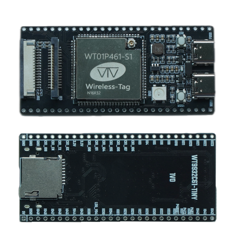
Note: The MIPI CSI/DSI interfaces use Raspberry Pi pin order. Carefully check the FPC direction and pin order before connecting a display or camera.
1. Introduction
WT9932P4C61-TINY is a mini development board designed for lightweight IoT development. It is based on Espressif ESP32-P4 + ESP32-C61 chips and uses the Wireless-Tag WT01P461-S1 module. With a compact 33 x 69 mm form factor, the board combines high-performance processing, wireless connectivity, and rich peripheral expansion. It is suitable for smart home products, low-power IoT terminals, HMI development, image display, and camera application validation.
The ESP32-P4 on the board runs at up to 400MHz and is suitable for display, image, USB, and general peripheral control tasks. The ESP32-C61 provides Bluetooth and Wi-Fi 6 dual-mode wireless communication. For hardware development, the board brings available pins out to 2.54mm pin headers for breadboard prototyping, and integrates serial flashing, an RGB indicator, EN and BOOT buttons, and a power indicator. The power section uses a DCDC design and supports up to 2A output current for stable peripheral power.
1.1 Core Hardware Configuration
- Core module: Wireless-Tag
WT01P461-S1module. - Main processor:
ESP32-P4, up to400MHz. - Wireless coprocessor:
ESP32-C61, supporting Bluetooth andWi-Fi 6dual-mode wireless communication. - Peripheral expansion: Onboard
MIPI CSI,MIPI DSI,MicroSDcard slot,USB Serial/JTAG, andUSB 2.0 OTG High-Speedinterfaces. - Pin headers:
J3andJ4dual-row2.54mmpin headers expose availableGPIOpins for breadboard or perfboard expansion. - Debug resources: Onboard
RESETbutton,BOOTbutton, andWS2812 RGB LED. - Power design: Powered through
USB Type-C, with onboardDCDCoutput up to2A. - Board size:
33 x 69 mm.
1.2 Design Features
- Dual-chip combination: Combines the high-performance processing capability of
ESP32-P4with the wireless connectivity ofESP32-C61, balancing performance and cost. - Onboard RGB indicator: The
WS2812 RGB LEDis connected toIO51and can be used for status indication and basic interaction tests. - Dual USB development interfaces: A
USB Type-Ccable can be used forP4andC61development and debugging. - EN and BOOT buttons: Onboard reset and download-mode buttons make it easy to manually enter flashing mode.
- Breadboard-friendly spacing: The pin headers use
2.54mmpitch for prototyping and peripheral expansion. - MIPI CSI/DSI interfaces: Camera and display interfaces use Raspberry Pi compatible pin order for display and image capture validation.
- Onboard MicroSD card slot: Supports a four-line
MicroSDcard interface for file systems, media resources, and data logging.
2. Hardware Peripherals
| Peripheral | Description |
|---|---|
WS2812 |
Single-wire RGB LED, connected to IO51 |
RESET button |
Used to reset the development board |
BOOT button |
Used to manually enter download mode, connected to IO35_BOOT |
FUSB |
Full-speed USB, used for power supply and firmware download/upgrade |
HUSB |
High-speed USB |
MIPI CSI FPC |
1.0mm pitch camera interface with Raspberry Pi pin order |
MIPI DSI FPC |
1.0mm pitch display interface with Raspberry Pi pin order |
MicroSD card |
Four-line MicroSD card interface |
2.1 Component Introduction
| No. | Component | Description |
|---|---|---|
J1 |
MIPI DSI Connector |
FPC connector for connecting an LCD expansion board. Compatible with 1.0mm pitch, 0.7mm pin width, 0.3mm thickness, and 15Pin FPC cables. |
J2 |
MIPI CSI Connector |
FPC connector for connecting an external camera module and transmitting image data. Compatible with 1.0mm pitch, 0.7mm pin width, 0.3mm thickness, and 15Pin FPC cables. |
J3, J4 |
2.54mm pin header interface |
All available GPIO pins are routed to pin headers J3 and J4, using 2.54mm pitch through-hole headers. |
J5 |
IPEX antenna socket |
Used to connect an external FPC antenna. |
J6 |
WS2812 RGB LED |
Single-wire interface, usable as an indicator LED. |
J7, J8 |
Tactile switches | Connected to RESET and BOOT. BOOT corresponds to IO35, which can be used as a normal button after boot. |
J9 |
USB Serial/JTAG Port |
USB Type-C interface supporting USB 2.0 Full-Speed. It can download firmware to ESP32-P4, communicate through the USB protocol, or be used for JTAG debugging. |
J10 |
USB 2.0 Type-C Port |
Connected to the ESP32-P4 USB 2.0 OTG High-Speed interface and compliant with the USB 2.0 standard. When used as a USB Host, it can provide up to 500mA externally. |
J11 |
MicroSD Card Slot |
Supports MicroSD cards in 4-bit mode. |
2.2 Interface Footprints
| Interface | Footprint | Remarks |
|---|---|---|
MIPI DSI FPC |
FPC_SMD_1.0K-FX-15PWBG |
Pay attention to the pin order |
MIPI CSI FPC |
FPC_SMD_15P-P1.00_HDGC_1.0K-GT-15PB |
Pay attention to the pin order |
MicroSD card interface |
MicroSD-SMD_MicroSD-PUSH |
Push-push card slot |
| Pin header x2 | HDR-TH_27P-P2.54-V-M |
Pitch supports perfboard/breadboard |
3. Pin Description
3.1 J1 MIPI DSI FPC
J1 is the MIPI DSI FPC interface, using 1.0mm pitch, 15Pin, drawer type, bottom contact, and horizontal mounting. Pay attention to the FPC pin order when using it.
| No. | Pin | Description | Voltage Range | Remarks |
|---|---|---|---|---|
| 1 | GND |
Power ground | 0V |
|
| 2 | DSI_DATAN1 |
DSI data lane 1 differential N |
0V/3.3V |
|
| 3 | DSI_DATAP1 |
DSI data lane 1 differential P |
0V/3.3V |
|
| 4 | GND |
Power ground | 0V |
|
| 5 | DSI_CLKN |
DSI clock differential N |
0V/3.3V |
|
| 6 | DSI_CLKP |
DSI clock differential P |
0V/3.3V |
|
| 7 | GND |
Power ground | 0V |
|
| 8 | DSI_DATAN0 |
DSI data lane 0 differential N |
0V/3.3V |
|
| 9 | DSI_DATAP0 |
DSI data lane 0 differential P |
0V/3.3V |
|
| 10 | GND |
Power ground | 0V |
|
| 11 | IO8 |
I2C SCL pin |
0V/3.3V |
|
| 12 | IO7 |
I2C SDA pin |
0V/3.3V |
|
| 13 | GND |
Power ground | 0V |
|
| 14 | VCC |
Power output | 3.3V |
Do not use as power input |
| 15 | VCC |
Power output | 3.3V |
Do not use as power input |
3.2 J2 MIPI CSI FPC
J2 is the MIPI CSI FPC interface, using 1.0mm pitch, 15Pin, drawer type, single-sided contacts, and vertical mounting. Pay attention to the FPC pin order when using it.
| No. | Pin | Description | Voltage Range | Remarks |
|---|---|---|---|---|
| 1 | GND |
Power ground | 0V |
|
| 2 | CSI_DATAN0 |
CSI data lane 0 differential N |
0V/3.3V |
|
| 3 | CSI_DATAP0 |
CSI data lane 0 differential P |
0V/3.3V |
|
| 4 | GND |
Power ground | 0V |
|
| 5 | CSI_DATAN1 |
CSI data lane 1 differential N |
0V/3.3V |
|
| 6 | CSI_DATAP1 |
CSI data lane 1 differential P |
0V/3.3V |
|
| 7 | GND |
Power ground | 0V |
|
| 8 | CSI_CLKN |
CSI clock differential N |
0V/3.3V |
|
| 9 | CSI_CLKP |
CSI clock differential P |
0V/3.3V |
|
| 10 | GND |
Power ground | 0V |
|
| 11 | IO1 |
Camera reset pin | 0V/3.3V |
|
| 12 | IO0 |
Unused pin | 0V/3.3V |
|
| 13 | IO8 |
I2C SCL pin |
0V/3.3V |
|
| 14 | IO7 |
I2C SDA pin |
0V/3.3V |
|
| 15 | VCC |
Power output | 3.3V |
Do not use as power input |
3.3 J9, J10 USB Type-C Interfaces
J9 and J10 are USB 2.0 Type-C interfaces and can be used for firmware download and power supply. J9 is a full-speed USB 2.0 interface with a maximum theoretical speed of 12Mbps, using IO24 and IO25. J10 is a high-speed USB 2.0 interface with a maximum theoretical speed of 480Mbps, using dedicated USB pins.
3.4 J11 MicroSD Card Interface
J11 is a push-push MicroSD card interface. Its power supply uses LDO_VO4, which can be configured to support 1.8V. Pull-ups also use LDO_VO4.
Note: Refer to the schematic and the official pin definition for the final
MicroSDsignal definitions.
| No. | Pin | Description | Voltage Range | Remarks |
|---|---|---|---|---|
| 1 | IO41 |
Four-line SDIO signal |
0V/LDO_VO4 |
|
| 2 | IO42 |
Four-line SDIO signal |
0V/LDO_VO4 |
|
| 3 | IO44 |
Four-line SDIO signal |
0V/LDO_VO4 |
|
| 4 | LDO_VO4 |
SD card power supply |
LDO_VO4 |
|
| 5 | IO43 |
Four-line SDIO signal |
0V/LDO_VO4 |
|
| 6 | GND |
Power ground | 0V |
|
| 7 | IO39 |
Four-line SDIO signal |
0V/LDO_VO4 |
|
| 8 | IO40 |
Four-line SDIO signal |
0V/LDO_VO4 |
3.5 J3, J4 Pin Header Interfaces
J3 and J4 are common 2.54mm pitch pin header interfaces.
J3 pin definition:
| No. | Pin | Description | Voltage Range | Remarks |
|---|---|---|---|---|
| 1 | GND |
Power ground | 0V |
|
| 2 | GND |
Power ground | 0V |
|
| 3 | GND |
Power ground | 0V |
|
| 4 | C61_IO9 |
C61 general-purpose input/output pin 9 / C61 BOOT pin |
0V/3.3V |
|
| 5 | C61_EN |
C61 reset enable pin |
0V/3.3V |
|
| 6 | C61_U0TXD |
C61 UART0 TX pin |
0V/3.3V |
|
| 7 | C61_U0RXD |
C61 UART0 RX pin |
0V/3.3V |
|
| 8 | 3.3V |
3.3V power output |
3.3V |
Do not input 3.3V |
| 9 | 3.3V |
3.3V power output |
3.3V |
Do not input 3.3V |
| 10 | C61_IO0 |
C61 general-purpose input/output pin 0 |
0V/3.3V |
|
| 11 | C61_IO1 |
C61 general-purpose input/output pin 1 |
0V/3.3V |
|
| 12 | C61_IO4 |
C61 general-purpose input/output pin 4 |
0V/3.3V |
|
| 13 | C61_IO5 |
C61 general-purpose input/output pin 5 |
0V/3.3V |
|
| 14 | C61_IO6 |
C61 general-purpose input/output pin 6 |
0V/3.3V |
|
| 15 | C61_IO7 |
C61 general-purpose input/output pin 7 |
0V/3.3V |
|
| 16 | C61_IO8 |
C61 general-purpose input/output pin 8 |
0V/3.3V |
|
| 17 | IO3 |
General-purpose input/output pin 3 | 0V/3.3V |
|
| 18 | IO4 |
General-purpose input/output pin 4 | 0V/3.3V |
|
| 19 | IO5 |
General-purpose input/output pin 5 | 0V/3.3V |
|
| 20 | IO6 |
General-purpose input/output pin 6 | 0V/3.3V |
|
| 21 | IO9 |
General-purpose input/output pin 9 | 0V/3.3V |
|
| 22 | IO10 |
General-purpose input/output pin 10 | 0V/3.3V |
|
| 23 | IO11 |
General-purpose input/output pin 11 | 0V/3.3V |
|
| 24 | IO20 |
General-purpose input/output pin 20 | 0V/3.3V |
|
| 25 | IO21 |
General-purpose input/output pin 21 | 0V/3.3V |
|
| 26 | IO22 |
General-purpose input/output pin 22 | 0V/3.3V |
|
| 27 | IO23 |
General-purpose input/output pin 23 | 0V/3.3V |
J4 pin definition:
| No. | Pin | Description | Voltage Range | Remarks |
|---|---|---|---|---|
| 1 | 5V |
5V power |
5V |
If J9 and J10 are both connected, the board internally prioritizes J9 for power supply |
| 2 | IO50 |
General-purpose input/output pin 50 | 0V/3.3V |
|
| 3 | IO49 |
General-purpose input/output pin 49 | 0V/3.3V |
|
| 4 | IO48 |
General-purpose input/output pin 48 | 0V/3.3V |
|
| 5 | IO47 |
General-purpose input/output pin 47 | 0V/3.3V |
|
| 6 | IO46 |
General-purpose input/output pin 46 | 0V/3.3V |
|
| 7 | IO45 |
General-purpose input/output pin 45 | 0V/3.3V |
|
| 8 | IO44 |
General-purpose input/output pin 44 | 0V/3.3V |
|
| 9 | IO43 |
General-purpose input/output pin 43 | 0V/3.3V |
|
| 10 | IO39 |
General-purpose input/output pin 39 | 0V/LDO_VO4 |
Can also be used as general input/output |
| 11 | LDO_VO4 |
SD card power output control pin |
LDO_VO4 |
Controls power for IO39-IO48 and can be configured by software |
| 12 | IO36 |
General-purpose input/output pin 36 | 0V/3.3V |
strapping pin |
| 13 | IO34 |
General-purpose input/output pin 34 | 0V/3.3V |
|
| 14 | IO31 |
General-purpose input/output pin 31 | 0V/3.3V |
|
| 15 | IO29 |
General-purpose input/output pin 29 | 0V/3.3V |
|
| 16 | IO28 |
General-purpose input/output pin 28 | 0V/3.3V |
|
| 17 | IO27 |
General-purpose input/output pin 27 | 0V/3.3V |
|
| 18 | IO26 |
General-purpose input/output pin 26 | 0V/3.3V |
|
| 19 | IO30 |
General-purpose input/output pin 30 | 0V/3.3V |
|
| 20 | IO32 |
General-purpose input/output pin 32 | 0V/3.3V |
|
| 21 | IO33 |
General-purpose input/output pin 33 | 0V/3.3V |
|
| 22 | IO35_BOOT |
General-purpose input/output pin 35 / BOOT pin |
0V/3.3V |
strapping pin |
| 23 | IO37_U0TXD |
General-purpose input/output pin 37 / UART 0TX pin |
0V/3.3V |
|
| 24 | IO38_U0RXD |
General-purpose input/output pin 38 / UART 0RX pin |
0V/3.3V |
|
| 25 | IO40 |
General-purpose input/output pin 40 | 0V/3.3V |
|
| 26 | IO41 |
General-purpose input/output pin 41 | 0V/3.3V |
|
| 27 | IO42 |
General-purpose input/output pin 42 | 0V/3.3V |
Note: After reset, the
strappingpin levels determine whether the board enters download mode.
| Boot Mode | GPIO35 |
GPIO36 |
GPIO37 |
GPIO38 |
|---|---|---|---|---|
SPI Boot |
1 | Any | Any | Any |
Joint Download Boot |
0 | 1 | Any | Any |
Note: The
TX0,RX0,EN, andBOOTsignals of theC61in the module are connected on the development board toC61pins 53, 54, 52, and 2 respectively.
4. Power Characteristics
The WT9932P4C61-TINY development board can be powered through a USB Type-C cable, and can also be connected to a computer USB port during debugging.
- Use a good-quality
USB-Ccable to ensure stable power supply. - If the board is powered from a computer
USBport, the port should provide at least5V@1A. - A
5V/1Aor higher power adapter is recommended. - The board power section uses a
DCDCdesign and supports up to2Aoutput current. - When
J10is used as aUSB Host, it can provide up to500mAexternally. - The
3.3Vpins on the headers are power outputs. Do not use them as3.3Vinputs. - The
MicroSDinterface power usesLDO_VO4, which can be configured to support1.8V.
If the UART connection appears and disappears after connecting FUSB, try holding the BOOT button, pressing the RESET button, and then releasing BOOT to manually enter download mode.