English
WT9932P4-TINY Feature Introduction
Update history
| Date | Version | Author | Update content |
|---|---|---|---|
| 2026-05-12 | 1.0.2 | Yobie Zhou | Added purchasing links |
| 2025-09-29 | 1.0.1 | Kirto | Added images and FPC pin sequence description |
| 2025-09-10 | 1.0.0 | Kirto | Initial document release |
⚠ Note: Due to power design, the FPC pin sequence is reversed compared to traditional Raspberry Pi. Carefully check the FPC pin sequence in the layout diagram when connecting.
1. Introduction
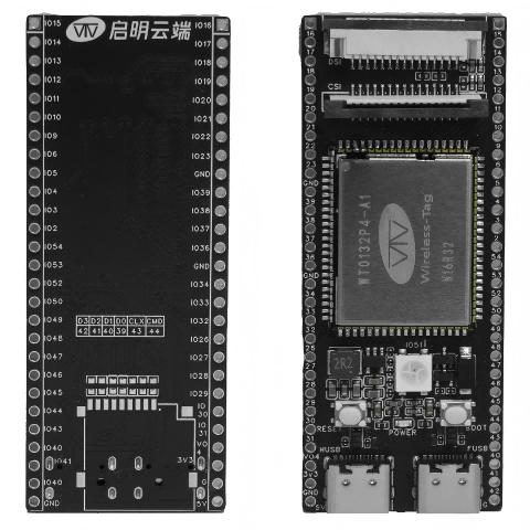
The WT9932P4-TINY from Wireless-tag's TINY open-source development board series is a pure microcontroller development board based on Espressif's ESP32-P4, focusing on compact and lightweight application scenarios. The ESP32-P4 is Espressif's new generation high-performance, low-power MCU, featuring a dual-core RISC-V processor with a maximum frequency of 400MHz, integrating rich peripherals and interface resources, supporting high-speed communication such as USB 2.0 OTG, MIPI CSI/DSI, SDIO, Ethernet, CAN FD, etc. It also includes built-in AI accelerator and graphics acceleration engine, capable of handling complex tasks like voice recognition, image processing, and edge computing. Its flexible storage expansion solution is compatible with PSRAM, external Flash, and large-capacity memory mapping, suitable for multi-tasking and large-scale application development. The design purpose of WT9932P4-TINY is to help developers quickly get started with ESP32-P4, providing a cost-effective, compact, and easy-to-learn-and-practice development platform in the open-source ecosystem.
Buy Now: WT9932P4-TINY Development Kit
1.1 🔧 Core Hardware Configuration
- Core Module: The development board uses Wireless-tag's WT0132P4-A1 module, which integrates core functions such as DCDC power supply, crystal oscillator, and Flash, greatly simplifying peripheral circuit design, allowing the development board to be designed with only two layers.
- MIPI Interface: The development board brings out MIPI CSI and MIPI DSI interfaces. The interfaces use the same pin sequence as Raspberry Pi, facilitating subsequent screen and camera development.
- SD Card Interface: The back of the development board supports 4-line SDIO. Users can solder and use the 4-line SD card interface themselves, making it convenient to use SD cards.
1.2 🛠️ Design Features
- Core Configuration: Centered around the high-performance Espressif ESP32P4 chip, meeting embedded development performance requirements.
- Compact Size: Only 69x28mm small specification, suitable for space-constrained application scenarios.
- Stable Design: Built based on the WT0132P4‑A1 module, using two-layer board design, ensuring stability while reducing costs.
- Image Interfaces: Onboard MIPI DSI and CSI FPC interfaces, supporting display output and image capture functions.
- Flexible Expansion: All pins are brought out, pin headers support breadboard connection, facilitating peripheral expansion.
- Status Indication: Equipped with onboard RGB LED, enabling multi-color status indication and interactive effects.
- Convenient Interfaces: Features Type‑C FUSB and HUSB interfaces, offering fast transmission and support for reversible plugging, convenient for debugging and power supply.
2. Pin Description
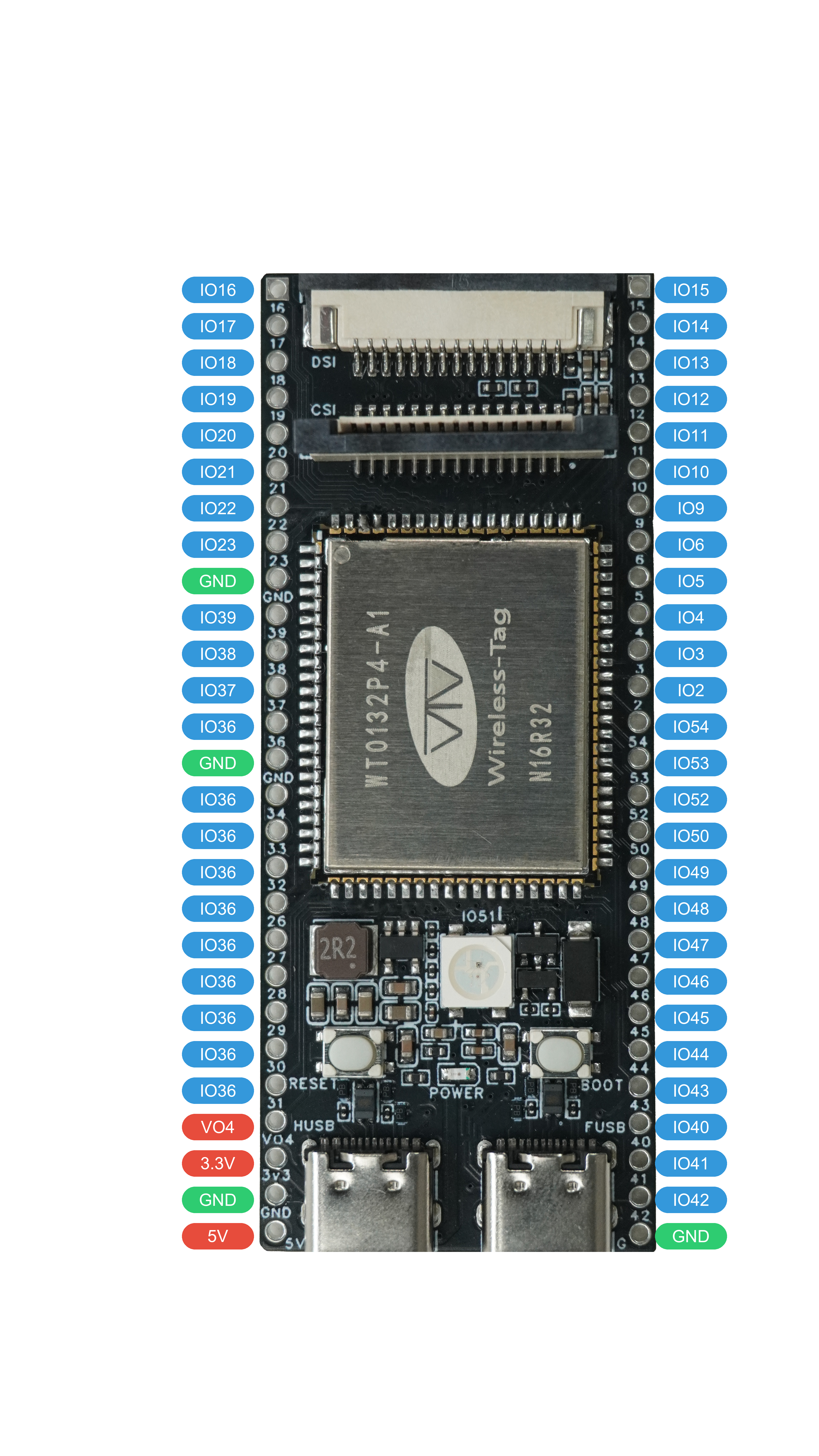
Left Pin Header:
| No. | Pin | Description | Voltage Range | Remarks |
|---|---|---|---|---|
| 1 | IO16 | General Purpose Input/Output Pin 16 | 0V/3.3V | |
| 2 | IO17 | General Purpose Input/Output Pin 17 | 0V/3.3V | |
| 3 | IO18 | General Purpose Input/Output Pin 18 | 0V/3.3V | |
| 4 | IO19 | General Purpose Input/Output Pin 19 | 0V/3.3V | |
| 5 | IO20 | General Purpose Input/Output Pin 20 | 0V/3.3V | |
| 6 | IO21 | General Purpose Input/Output Pin 21 | 0V/3.3V | |
| 7 | IO22 | General Purpose Input/Output Pin 22 | 0V/3.3V | |
| 8 | IO23 | General Purpose Input/Output Pin 23 | 0V/3.3V | |
| 9 | GND | Power Ground | 0V | |
| 10 | IO39 | SD Card DATA0 Pin | 0V/LDO_VO4 | Can also be used as general input/output |
| 11 | IO38 | UART0 RXD Pin, for debugging or flashing | 0V/3.3V | Strapping pin |
| 12 | IO37 | UART0 TXD Pin, for debugging or flashing | 0V/3.3V | Strapping pin |
| 13 | IO36 | General Purpose Input/Output Pin 36 | 0V/3.3V | Strapping pin |
| 14 | GND | Power Ground | 0V | |
| 15 | IO34 | General Purpose Input/Output Pin 34 | 0V/3.3V | |
| 16 | IO33 | General Purpose Input/Output Pin 33 | 0V/3.3V | |
| 17 | IO32 | General Purpose Input/Output Pin 32 | 0V/3.3V | |
| 18 | IO26 | General Purpose Input/Output Pin 26 | 0V/3.3V | |
| 19 | IO27 | General Purpose Input/Output Pin 27 | 0V/3.3V | |
| 20 | IO28 | General Purpose Input/Output Pin 28 | 0V/3.3V | |
| 21 | IO29 | General Purpose Input/Output Pin 29 | 0V/3.3V | |
| 22 | IO30 | General Purpose Input/Output Pin 30 | 0V/3.3V | |
| 23 | IO31 | General Purpose Input/Output Pin 31 | 0V/3.3V | |
| 24 | LDO_VO4 | SD Card Power Supply Pin | LDO_VO4 | |
| 25 | 3.3V | 3.3V Power Output | 3.3V | Do not input 3.3V |
| 26 | GND | Power Ground | 0V | |
| 27 | 5V | 5V Power Supply | 5V | If both J3 and J4 are connected, J3 has priority for internal power supply |
Right Pin Header:
| No. | Pin | Description | Voltage Range | Remarks |
|---|---|---|---|---|
| 1 | IO15 | General Purpose Input/Output Pin 15 | 0V/3.3V | |
| 2 | IO14 | General Purpose Input/Output Pin 14 | 0V/3.3V | |
| 3 | IO13 | General Purpose Input/Output Pin 13 | 0V/3.3V | |
| 4 | IO12 | General Purpose Input/Output Pin 12 | 0V/3.3V | |
| 5 | IO11 | General Purpose Input/Output Pin 11 | 0V/3.3V | |
| 6 | IO10 | General Purpose Input/Output Pin 10 | 0V/3.3V | |
| 7 | IO9 | General Purpose Input/Output Pin 9 | 0V/3.3V | |
| 8 | IO6 | General Purpose Input/Output Pin 6 | 0V/3.3V | |
| 9 | IO5 | General Purpose Input/Output Pin 5 | 0V/3.3V | Also JTAG MTCK pin |
| 10 | IO4 | General Purpose Input/Output Pin 4 | 0V/3.3V | Also JTAG MTDI pin |
| 11 | IO3 | General Purpose Input/Output Pin 3 | 0V/3.3V | Also JTAG MTMS pin |
| 12 | IO2 | General Purpose Input/Output Pin 2 | 0V/3.3V | Also JTAG MTCK pin |
| 13 | IO54 | General Purpose Input/Output Pin 54 | 0V/3.3V | |
| 14 | IO53 | General Purpose Input/Output Pin 53 | 0V/3.3V | |
| 15 | IO52 | General Purpose Input/Output Pin 52 | 0V/3.3V | |
| 16 | IO50 | General Purpose Input/Output Pin 50 | 0V/3.3V | |
| 17 | IO49 | General Purpose Input/Output Pin 49 | 0V/3.3V | |
| 18 | IO48 | SD Card DATA7 Pin | 0V/LDO_VO4 | Can also be used as general input/output |
| 19 | IO47 | SD Card DATA6 Pin | 0V/LDO_VO4 | Can also be used as general input/output |
| 20 | IO46 | SD Card DATA5 Pin | 0V/LDO_VO4 | Can also be used as general input/output |
| 21 | IO45 | SD Card DATA4 Pin | 0V/LDO_VO4 | Can also be used as general input/output |
| 22 | IO44 | SD Card CMD Pin | 0V/LDO_VO4 | Can also be used as general input/output |
| 23 | IO43 | SD Card CLK Pin | 0V/LDO_VO4 | This pin as ordinary IO is output only |
| 24 | IO40 | SD Card DATA1 Pin | 0V/LDO_VO4 | Can also be used as general input/output |
| 25 | IO41 | General Purpose Input/Output Pin 41 | 0V/3.3V | |
| 26 | IO42 | General Purpose Input/Output Pin 42 | 0V/3.3V | |
| 27 | GND | Power Ground | 0V |
3. Power Characteristics
You can choose one of the following power supply methods for the WT9932P4-TINY series development board:
- External power supply via the
FUSBinterface; - External power supply via the
HUSBinterface; - Use the
5Vpower input port and connect the corresponding voltage via Dupont wires;